 |
|
LC feedback are used in oscillators that require higher frequency and higher Q factor. Transistors are used as amplifiers because of the limitation (lower unity-gain frequency) of Op-amps. There are four types of LC oscillators, Armstrong, Clapp, Hartley, Colpitts. The benefits of LC oscillators are phase stability and low susceptibility to noise. LC oscillators have a higher Q factor than Relaxation oscillators. However, they have lower tuning range and higher cost compare to Relaxtion oscillators. A LC oscillator in which dc power is supplied to the transistor through the tank circuit, or a portion of the tank circuit, is said to be SERIES FED. A LC oscillator which receives its dc power for the transistor through a path that is separate and parallel to the tank circuit is said to be PARALLEL FED OR SHUNT FED. All the LC oscillators for this article can be constructed either way, series or shunt fed. Armstrong Oscillator The armstrong oscillator uses transformer coupling to feed back a portion of the amplifier output to the amplifier input. It is used less often then the other LC oscillators because of the transformer size and cost.
Fig 1
Fig 2
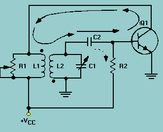
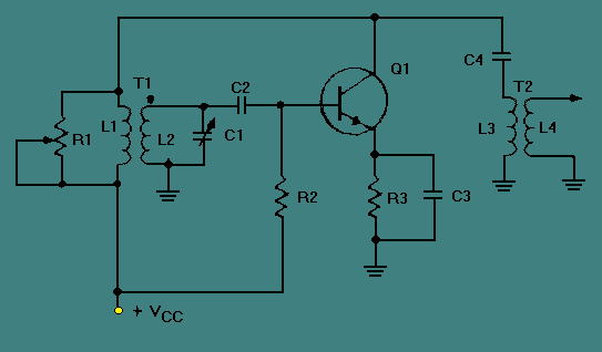
Fig 3 The circuit in Fig3 has all three requirements for an oscillator: (1) amplification, (2) a frequency-determining device, and (3) regenerative feedback. The oscillator in this schematic drawing is a tuned-base oscillator, because the fdd is in the base circuit. If the fdd were in the collector circuit, it would be a tuned-collector oscillator. When VCC is applied to the circuit. a small amount of base current flows through R2 which sets the forward bias on Q1. This forward bias causes collector current to flow from ground through Q1, R1, and L1 to +VCC. The current through L1 develops a magnetic field which induces a voltage into the tank circuit. The voltage is positive at the top of L2 and C1. At this time, two actions occur. First, resonant tank capacitor C1 charges to this voltage; the tank circuit now has stored energy. Second, coupling capacitor C2 couples the positive signal to the base of Q1. With a positive signal on its base, Q1 conducts harder. With Q1 conducting harder, more current flows through L1, a larger voltage is induced into L2, and a larger positive signal is coupled back to the base of Q1. While this is taking place, the frequency-determining device is storing more energy and C1 is charging to the voltage induced into L2. The transistor will continue to increase in conduction until it reaches saturation. At saturation, the collector current of Q1 is at a maximum value and cannot increase any further. With a steady current through L1, the magnetic fields are not moving and no voltage is induced into the secondary. With no external voltage applied, C1 acts as a voltage source and discharges. As the voltage across C1 decreases, its energy is transferred to the magnetic field of L2. Now, let's look at C2. The coupling capacitor, C2, has charged to approximately the same voltage as C1. As C1 discharges, C2 discharges. The primary discharge path for C2 is through R2 (shown by the dashed arrow). As C2 discharges, the voltage drop across R2 opposes the forward bias on Q1 and collector current begins to decrease. This is caused by the decreasing positive potential at the base of Q1. A decrease in collector current allows the magnetic field of L1 to collapse. The collapsing field of L1 induces a negative voltage into the secondary which is coupled through C2 and makes the base of Q1 more negative. This, again, is regenerative action; it continues until Q1 is driven into cutoff. When Q1 is cut off, the tank circuit continues to flywheel, or oscillate. The flywheel effect not only produces a sine-wave signal, but it aids in keeping Q1 cut off. Without feedback, the oscillations of L2 and C1 would dampen out after several cycles. To ensure that the amplitude of the signal remains constant, regenerative feedback is supplied to the tank once each cycle, as follows: As the voltage across C1 reaches maximum negative, C1 begins discharging toward 0 volts. Q1 is still below cutoff. C1 continues to discharge through 0 volts and becomes positively charged. The tank circuit voltage is again coupled to the base of Q1, so the base voltage becomes positive and allows collector current to flow. The collector current creates a magnetic field in L1, which is coupled into the tank. This feedback action replaces any lost energy in the tank circuit and drives Q1 toward saturation. After saturation is reached, the transistor is again driven into cutoff. The operation of the Armstrong oscillator is basically this: Power applied to the transistor allows energy to be applied to the tank circuit causing it to oscillate. Once every cycle, the transistor conducts for a short period of time (Class C operation) and returns enough energy to the tank to ensure a constant amplitude output signal. Class C operation has high efficiency and low loading characteristics. The longer Q1 is cut off, the less the loading on the frequency-determining device. Figure 4 shows a tuned-base Armstrong oscillator as you will probably see it. R3 has been added to improve temperature stability. Bypass capacitor C3 prevents degeneration. C4 is an output coupling capacitor, and impedance-matching transformer T2 provides a method of coupling the output signal. T2 is usually a loosely coupled rf transformer which reduces undesired reflected impedance from the load back to the oscillator.
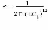
Fig 4 For circuits in the 400 to 2000 MHz range, modern oscillators tend to use transmission-line resonators and capacitive feedback of the Colpitts or Clapp type. Colpitts Oscillator The colpitts oscillator uses a pair of tapped capacitors and an inductor to produce the regenerative feedback nesessary for oscillation. The amplifier output is developed across C1, and feedback voltage is developed across C2. The voltage across C2 is 180 degrees out of phase with the voltage across C1, thus feedback is regenerative. . Resistors, R1 and R2 provide the usual stabilizing DC bias for the transistor in the normal manner while the capacitor acts as a DC-blocking capacitors. Fig 5 The frequency of oscillations for a Colpitts Oscillator is determined by the resonant frequency of the LC tank circuit and is given as:
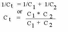
where CT is the capacitance of C1 and C2 connected in series and is given as:
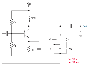
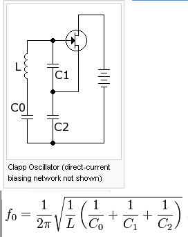
The configuration of the transistor amplifier is of a Common Emitter Amplifier with the output signal 180 degrees out of phase with regards to the input signal. Both the Armstrong and the Hartley oscillators have a tendency to be unstable in frequency because of junction capacitance. In comparison, the colpitts oscillator has fairly good frequency stability, is easy to tune, and can be used for a wide range of frequencies. The large value of split capacitance is in parallel with the junctions and minimizes the effect on frequency stability. .Clapp Oscillator The Clapp oscillator is simply a Colpitts oscillator with an extra capacitor in series with the coil. It is labeled as C3 in Fig 6. The function of C3 is to reduce the effects of junction capacitance on operating frequency. C1 is in parallel with the Miller input capacitance, Cin(M). C3 is always much lower in value than either C1 or C2, so it becomes the dominant capacitor in any frequency calculation. The reason we still need C1 and C2 is to provide the phase shift needed for regenerative feedback. C3 has not replaced C1 and C2. It is simply there to determine the operating frequency. Since C1 and C2 are eliminated from the frequency calculation, junction capacitance has little or no effect on operating frequency. Advantages of Clapp Oscillators Because there is no load on the inductor a high "Q" circuit results with a high L/C ratio and of course much less circulating current. This aids drift reduction. Because larger inductances are required, stray inductances do not have as much impact as perhaps in other circuits. The additional capacitor offers more accurate and stable frequency compared to Hartley and Colpitts oscillators. It has the added advantage of a higher loaded Q factor than the Colpitts.
Fig 6
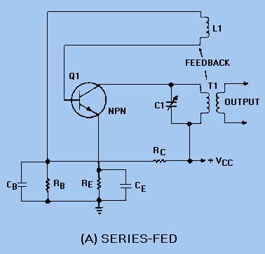
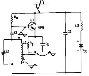
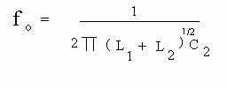
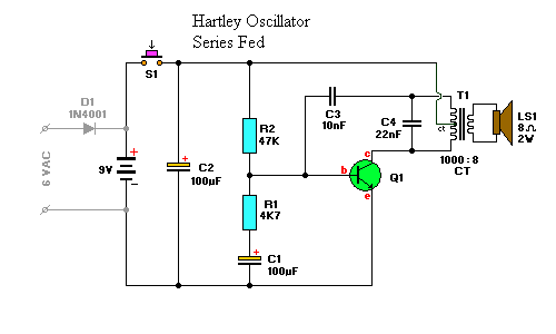
Fig 7 A Clapp circuit is often preferred over a Colpitts circuit for constructing a variable frequency oscillator (VFO). In a Colpitts VFO, the voltage divider contains the variable capacitor (either C1 or C2). This causes the feedback voltage to be variable as well, sometimes making the Colpitts circuit less likely to achieve oscillation over a portion of the desired frequency range. This problem is avoided in the Clapp circuit by using fixed capacitors in the voltage divider and a variable capacitor (C0) in series with the inductor. Hartley Oscillator The hartley oscillator is similar to the colpitts oscillator. It uses a pair of tapped inductors and capacitor to produce the regenerative feedback nesessary for oscillation. It has the advantage of having its output amplitude remain constant (amplitude stability) over a tunable frequency range.However, it generates harmonics frequencies which prevents it from producing pure sine waves. The hartley oscillator is an improvement over the Armstrong oscillator. Although its frequency stability is not the best possible of all the oscillators, the Hartley oscillator can generate a wide range of frequencies and is very easy to tune. The Hartley will operate Class C with self-bias for ordinary operation. It will operate Class A when the output waveform must be of a constant voltage level or of a linear waveshape. Advantages of Hartley Oscillators The frequency is simply varied by the net value of C in the tank circuit. The output amplitude remains constant when tuned over the frequency range. The feedback ratio of L1 to L2 (figure 1) remains constant. Disadvantages of Hartley Oscillators The output is rich in harmonic content and therefore not suitable where a pure sine wave is required. Series-Fed One version of a SERIES-FED hartley oscillator is shown in figure 8. The tank circuit consists of the tapped coil (L1 and L2) and capacitor C2. The feedback circuit is from the tank circuit to the base of Q1 through the coupling capacitor C1. Coupling capacitor C1 prevents the low dc resistance of L2 from placing a short across the emitter-to-base junction and resistor RE. Capacitor C3 bypasses the sine-wave signal around the battery, and resistor RE is used for temperature stabilization to prevent thermal runaway. Degeneration is prevented by CE in parallel with RE. The amount of bias is determined by the values of RB, the emitter-to-base resistance, the small amount of dc resistance of coil L1, and the resistance of RE.
Fig. 8
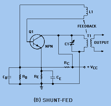
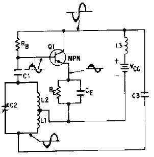
Shunt Fed A version of a SHUNT-FED hartley oscillator is shown in figure 9. The parts in this circuit perform the same basic functions as do their counterparts in the series-fed Hartley oscillator. The difference between the series-fed and the shunt-fed circuit is that dc does not flow through the tank circuit. The shunt-fed circuit operation is essentially the same as the series-fed Hartley oscillator. When voltage is applied to the circuit, Q1 starts conducting. As the collector current of Q1 increases, the change (increase) is coupled through capacitor C3 to the tank circuit, causing it to oscillate. C3 also acts as an isolation capacitor to prevent dc from flowing through the feedback coil. The oscillations at the collector will be coupled through C3 (feedback) to supply energy lost within the tank.
Fig 9 Application: Doorbell
|
|
|
|
Contact email: qooljaq@qooljaq.com |